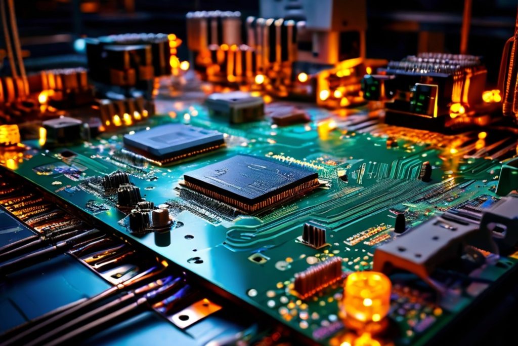
The Manufacturing Process of PCBs: Steps and Technical Requirements
Understanding the Complex Craft of PCB Production

Printed Circuit Boards (PCBs) serve as the backbone of modern electronics. They connect various components, like microcontrollers and sensors, enabling devices to function seamlessly. The manufacturing of PCBs involves several critical steps, each with specific technical requirements.
First, designers create a schematic layout using software tools. For instance, engineers at a smartphone company design circuits that manage battery life and connectivity. After finalizing the layout, they transfer it onto a laminate using a process called photolithography. This technique involves applying a light-sensitive film to the copper-clad laminate, exposing it to UV light, and developing the image to reveal the circuit patterns. Consequently, businesses can produce intricate designs that meet user demands.
Next, manufacturers etch the exposed copper away using a chemical process. This step ensures that only the desired circuit remains, creating pathways for electricity. For example, manufacturers can produce PCBs for medical devices, where precise circuit paths are crucial for monitoring patient health. After etching, they drill holes for component placement and plating, which adds layers of conductive material to ensure reliable connections.
Moreover, solder mask application comes next. This layer protects the PCB from environmental factors and prevents short circuits. For example, in automotive electronics, durable solder masks are vital for components that endure harsh conditions. Following this, manufacturers print silkscreen labels to indicate component placements, ensuring that assembly workers can easily identify where each part fits.
Quality control plays a significant role throughout the PCB manufacturing process. Inspectors test each board for defects, ensuring reliability. For instance, PCBs in aerospace applications undergo rigorous testing to meet high safety standards. Once approved, manufacturers package the PCBs, ready for integration into consumer products, such as laptops and game consoles.
In summary, the manufacturing process of PCBs encompasses design, etching, drilling, and quality control. These steps highlight the intricate work involved in producing PCBs that power everyday devices. Thus, understanding these processes enriches our appreciation for the technology that drives our daily lives.
Ready to elevate your project with us? Reach out to us now and let’s make it happen!
